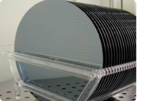
Advantage of our products:
    1. Metal film Wafers, such as Al, Ni, Ag, Au, Ti, Pt, wafers, platted with 99.99% + or 99.995% +, plasma. 2. 100% pass peeling test before delivery. No peeling problem.
Application:
1. Packaging test. 2. Lapping test. 3. Cutting test.
4. Wafer mounting test. 5. Wire bonding test.
6.Quality control of the machine / Setting of parameter test.
7. Special experiment/ proofing
8. Dummy IC/chips producing
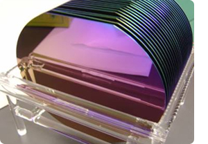
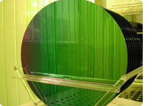
6” 8” 12” Aluminum wafer
6”Aluminum wafer
Thickness (µ m) ≧500     
TTV (µ m)    ≦50um   
WARP (µ m)    ≦50um    
Metallization Thinkness   1000~10000A± 10%  
8”Aluminum wafer
Thickness (µ m) ≧600     
WARP (µ m)    ≦50um    
TTV (µ m)    ≦50um   
Metallization Thinkness   1000~10000A± 10%  
12”Aluminum wafer
Thickness (µ m) ≧650     
WARP (µ m)    ≦50um    
TTV (µ m)    ≦50um   
Metallization Thinkness  1000~10000A± 10%  
 

Thermal Oxide wafer
Application:
1. Etch rate test. 2. Metal bonding test
3. Electric insulation layer
6” & 8” & 12” Thermal Oxide Wafer
6”Thermal Oxide Wafer
Thickness (µ m) 675 ± 25 um     
Type P
Orientation <100>
Res.; 1 ~ 100 ohm-cm
TTV (µ m)    ≦50um   
WARP (µ m)    ≦50um    
Metallization Thinkness   1000~10000A± 10%  
8”Thermal Oxide Wafer
Thickness (µ m) 725 ± 25 um     
Type P
Orientation <100>
Res.; 1 ~ 100 ohm-cm
TTV (µ m)    ≦50um   
WARP (µ m)    ≦50um    
Metallization Thinkness   1000~10000A± 10%  
12” Thermal Oxide Wafer
Thickness (µ m) 775 ± 25 um     
Type P
Orientation <100>
Res.; 1 ~ 100 ohm-cm
TTV (µ m)    ≦50um   
WARP (µ m)    ≦50um    
Metallization Thinkness   1000~10000A± 10%  
 

Thinning wafer
Extra flat/ Extra thin/ Thinning service